Industry Directory | Consultant / Service Provider / Manufacturer
Taiwan's leading design and manufacturing agency dealing with PCB and IC. Tech: Up to 40 layers, 2 Mill trace width .3" thickness. Global clientele, 11 years engineering, American/British staff.
Industry Directory | Manufacturer
Innovative Sensor Technology is a manufacturer of thin-film platinum and nickel RTD temperature sensors, capacitive humidity sensors, mass flow sensors, conductivity and biosensors.
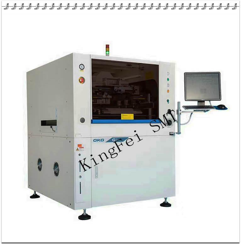
New Equipment | Assembly Services
G9 + automatic vision printing machine is a new product for SMT high-end application field, which can perfectly meet the process requirements of 03015, 0.25pich and other fine spacing, high precision and high speed. Introduction to standard function
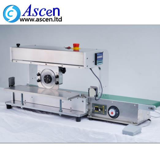
After soldering the PCBA plate of connecting pieces, it often hurts lines or breaks the electronic parts when breaking. This pcb depaneling machine cuts PCBA with feed mode to reduce stress drastically, prevent the solder joint and parts from crackin
Electronics Forum | Sat Sep 04 11:58:44 EDT 2004 | Dhanashekar
Can anyone suggest me if it is necessary to measure the paste thickness after contact Screen printing.Is it a very vital parameter for the production process?
Electronics Forum | Sat Sep 04 18:52:51 EDT 2004 | iqbalb
Yes it is vital for process control.
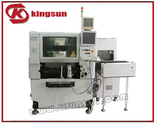
Used SMT Equipment | SMT Equipment
Product name: KE - 2060 l JUKI chip mounter Product number: KE - 2060 l JUKI2060 chip mounter parameters: Mounting head: 3 Material stand: 80 Mount speed: 0.25 SEC/CHIP (3 head at the same time put in the attached SMT) Mounting speed:+ / - 0.
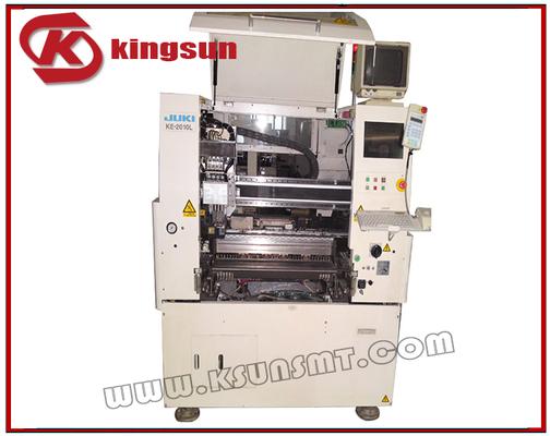
Used SMT Equipment | SMT Equipment
Product name: KE - 2010 l JUKI chip mounter Product number: KE - 2010 l Products in detail Substrate size: Min: 50 mmx30mm Max: 330 mmx250mm Substrate thickness: Min: 0.4 mm Max: 4 mm Element size: 0402 ~ 20 mm square element or 26.5 X11mm Mo
Industry News | 2023-10-16 12:50:01.0
MIRTEC announces the release of their All-New ART Hybrid 3D AOI System at Productronica 2023. The World's leading trade fair for the electronics manufacturing industry will take place Nov. 14-17, 2023, at the Trade Fair Center Messe München, Germany. All are welcome to MIRTEC's Booth #461 in Hall A2 for a detailed demonstration of what will undoubtedly be recognized as the World's Most Technologically Advanced 3D AOI System!
Industry News | 2010-12-17 01:47:04.0
IPC has released the A revision of IPC-2222, Sectional Design Standard for Rigid Organic Printed Boards. Helping developers avoid common missteps that reduce board manufacturability, IPC-2222 has been expanded to include more information on board materials, such as relative costs, tolerances of board thickness, unsupported holes, and hole aspect ratios.

Parts & Supplies | SPI / Solder Paste Inspection
Quick programming, friendly programming interface Multiple measurement methods True one-button measurement Eight-way motion button, one-click focus Adjustable scanning pitch Solder paste 3D simulation function Powerful SPC function MARK
.jpg)
Parts & Supplies | Assembly Accessories
We can bring you the following benefits. 1. Save costs 2. MOQ:1 pc 3. You can find the SMT parts you want 4. Fast delivery-- receive the goods in about 7 days 5. Sincere one-to-one professional service 6. Quick response after-sales service Ple
Technical Library | 2013-10-13 10:54:13.0
The measurement of the conformal coating thickness on a printed circuit board (PCB) to ensure internal and international standards are met is now a critical factor in conformal coating process control. There are several methods for measurement of conformal coating thickness and they fall into two categories. These categories are wet film measurements applied during coating application and dry film measurements made after the coating is dried enough not to damage the coating.
Technical Library | 2020-07-22 19:39:05.0
The PWB industry needs to complete reliability testing in order to define the minimum copper wrap plating thickness requirement for confirming the reliability of PTH structures. Predicting reliability must ensure that the failure mechanism is demonstrated as a wear-out failure mode because a plating wrap failure is unpredictable. The purpose of this study was to quantify the effects of various copper wrap plating thicknesses through IST testing followed by micro sectioning to determine the failure mechanism and identify the minimum copper wrap thickness required for a reliable PWB. Minimum copper wrap plating thickness has become an even a bigger concern since designers started designing HDI products with buried vias, microvias and through filled vias all in one design. PWBs go through multiple plating cycles requiring planarization after each plating cycle to keep the surface copper to a manageable thickness for etching. The companies started a project to study the relationship between Copper wrap plating thickness and via reliability. The project had two phases. This paper will present findings from both Phase 1 and Phase 2.
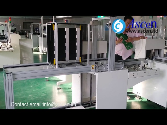
PCB magazine unloader/Multi magazine unloader how to receive the PCB after soldering, more detail check :https://www.ascen.ltd/Products/Automatic_SMT_equipment/PCB_loader/91.html Multi Magazine PCB unloader is used at the end of the SMT line for unlo

Manual V Cut PCB Depanelizer PCB Board Cutter It is widely used in modern rigid PCB industry. Manual V Cut PCB Depanelizer Machine Features: 1. Simple operation, speed is fast, to ensure that components of substrate are not injured by the move
Career Center | Chesterland, Ohio USA | Production
Surface Grinder/Lapper Operator Position Overview We currently have an excellent career opportunity for a Surface Grinder/Lapper Operator to join our Ceramics team at our Channel Products, Inc. facility in Chesterland, OH. This position is respons
Career Center | Theni, Tamilnadu India | Engineering
NPI Engineer: • Playing a role as NPI leader of the Telecom, Aerospace & Server Products to introduce and run to qualify the engineering build from customer. • Conducting Weekly NPI meeting with the CFT team to review the progress of the NPI schedu
Career Center | Erode, Tamilnadu India | Engineering
Professional Summary 3+ years of experience in the PCB CAM engineering Exposure to FRONTLINE GENESIS 2000 Having exposure in UCAM Exposure to Create, Array & Panelize it for manufacturability Experienced in Creating impedance cou
Influence of Pd Thickness on Micro Void Formation of Solder Joints in ENEPIG Surface Finish SMTnet Express December 13, 2012, Subscribers: 26067, Members: Companies: 9068, Users: 34058 Influence of Pd Thickness on Micro Void Formation of Solder
| https://ipcapexexpo.org/exhibitors/general-artwork-format-specifications
— manipulation of images must be allowed All fonts must be converted to outlines Outline thickness no less than 1 point Type no less than 8 points Send all artwork to KimDiCianni@ipc.org Logo example
| http://etasmt.com/cc?ID=te_news_industry,6361&url=_print
. After the placement is completed, it is necessary to adjust the position and judge the direction, and take effective measures to do laser recognition and camera recognition


